| CCDSP | Silicon DSP Corporation | CCDSP Tech Blog |
April 1991
Original Scanned Document in PDF.
Note: The HTML for this report was created from the scanned document by CCDSP using OCR (Acrobat Pro), Latex and Snagit. Original report based on Final Project Report in Advanced Communications Graduate Course, NC State University taught by Professor Sasan Ardalan.
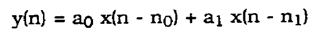
In this project, a baseband digital communications link was investigated. In particular, two important issues, timing recovery and channel equalization, were explored. A popular technique for timing wave extraction was examined both theoretically and throgh simulation. An adaptive equalizer was designed to compensate for common channel distortions. Both a lowpass and a multipath channel were simulated.
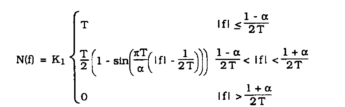
Figure 1 shows the CAPSIM topology used to perfrom the timing recovery simulations. The binary data signal is transmitted through a pulse shaping filtyer with a square-root Nyquist spectral response. The optimum matched filter has the same response. The overall pulse spectrum, NF, has the Nyquist spectral response characteristic eliminating inter-symbol interference (ISI) over bandlimited channels. N(f) is given by,
 (1)
(1)
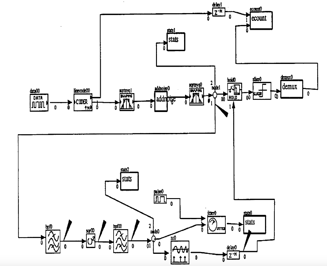
Figure 1 Timing Recovery Topology
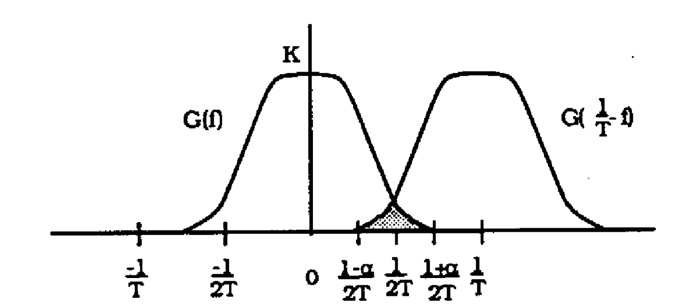
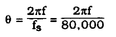
where 1/T = 1000 Hz: the data rate of our system. and alpha is the coefficient of excess bandwidth. The sampling rate of the system is 8000 Hz. The recovered pulse is passed through a prefilter. The filter response of the prefilter, H(f) is determined such that the spectrum of the resulting signal is symmetrical about half the bit rate, 500 Hz. The reasons for this are discussed later. Figure 2 shows the spectrwn of the prefilter output signal when 100% excess bandwidth is used in the pulse shaping filters (alpha= 1.0).
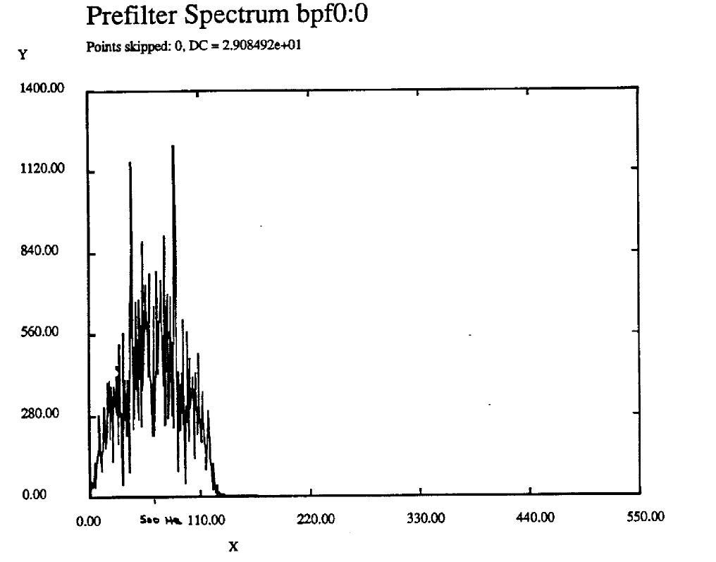
Figure 2. Spectrum of Prefilter Output ALPHA=1.0
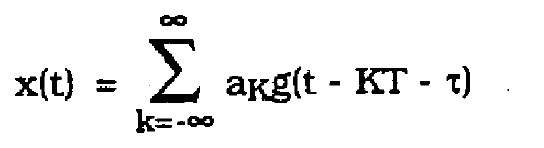
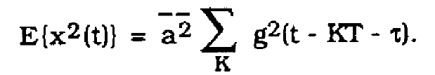
The output of the prefllter is passed through a squaring circuit. Denote the signal at the output of the squaring circuit as x(t). For binary baseband transmission, x(t) can be written by,
 (2)
(2)
where ![]() is the binary symbol set and g(t) is the impulse response of the system through the prefilter. In [1], Franks shows that,
is the binary symbol set and g(t) is the impulse response of the system through the prefilter. In [1], Franks shows that,
 (3)
(3)
Equation {3} relies on the fact that for stationary, independent binary
signals,
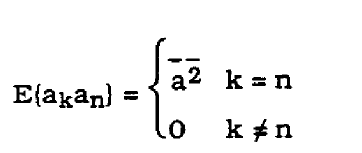 (4)
(4)
Using the Poisson sum formula, Franks shows in [2] that ![]() can be expressed by,
can be expressed by,
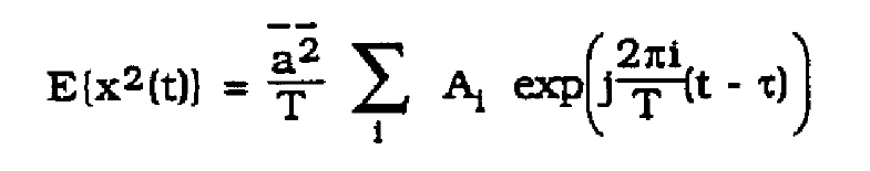 (5)
(5)
where
 (6)
(6)
and g(t} <-->G(f). For Nyquist pulse shaping. only ![]() exist. Examining the sum of complex exponentials in (5) it is evident that spectral
exist. Examining the sum of complex exponentials in (5) it is evident that spectral
components exist at DC and at f = 1/T. A sinusoid at f =1/T is the desired timing wave.
Figure 3 shows the spectrum at the output of the squaring circuit for 100% excess bandwidth and prefiltering.
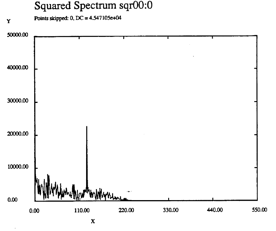
Figure 3 Spectrum of Squared Signal ![]() , alpha =1.0 Prefiltered.
, alpha =1.0 Prefiltered.
The output of the squaring circuit is passed through a high-Q bandpass filter H2(f) tuned to f=1/T. This filter recovers the spectral component of ![]() at f=1/T. Denote the output of this filter as w(t) . In [2], Franks shows that the signal w(t) is cyclostationary with period 1/T . The mean of w(t) can be given by (7) including
at f=1/T. Denote the output of this filter as w(t) . In [2], Franks shows that the signal w(t) is cyclostationary with period 1/T . The mean of w(t) can be given by (7) including ![]() terms.
terms.
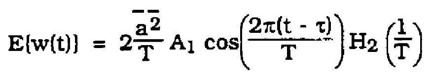 (7)
(7)
The mean of w(t) has the desired properties of a timing wave. However, the zero crossings of w(t) are used to recover the receiver timing clock. The
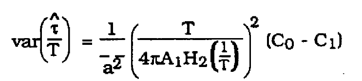
key figure of merit for timing recovery systems is the variance in the zero crossing phase of w{t), denoted as ![]() , in relation to the pulse period T. This is the Jitter variance of the timing signal.
, in relation to the pulse period T. This is the Jitter variance of the timing signal.
An expression for the jitter variance of the tlming wave, denoted as  is desired. Expressions for timing Jitter in the presence of additive noise are difficult to develop. Normally the jitter variance of design interest is pattern-dependent jitter which depends on the statistics of the binary data.
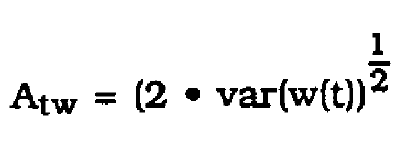
It has been demonstrated in [3] that the timing jitter variance will decrease in proportion to increasing mean slope of the timing wave w(t) at its zero crossings, and thus be inversely proportional to the amplitude of w{t). In {2] Franks gives a will popular approximation for pattern-dependent timing jitter ( assuming H2(1/T)=1),
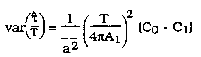 (8)
(8)
where Co and C 1 are constants which depend on the spectrums G(f) and H2(f) in a complicated way. For the rest of the analysis, it is assumed that Co
and C 1 are undetermined constants. It is clear from (8) that timing Jitter is inversely proportional to the square of the timing wave amplitude.
An interesting result shown in [1] is that Co = C1 when certain spectral symmetries are observed, i. e. if G(fl is symmetrical about f = 1/2T and H2 (f) is
symmetrical about 1/T . In this case, the timing jitter vanishes. The symmetry condition on H2(f) is usually attempted in the high-Q filter design. The symmetry condition for G(f) is not met by Nyquist pulse shaping; this is why
the prefilter H2(0 1s included. In the absence of a preftlter, the jitter
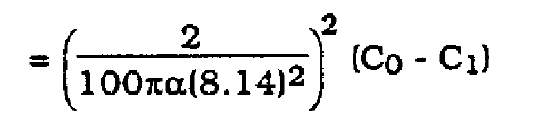
variance will be inversely proportional to the square of A1 (assuming Co, C1 fixed). A1 depends linearly on the excess bandwidth constant alpha, as is developed below for Nyquist pulse shaping.
Ai given by (6) for i = 1. G(f) given by (1)
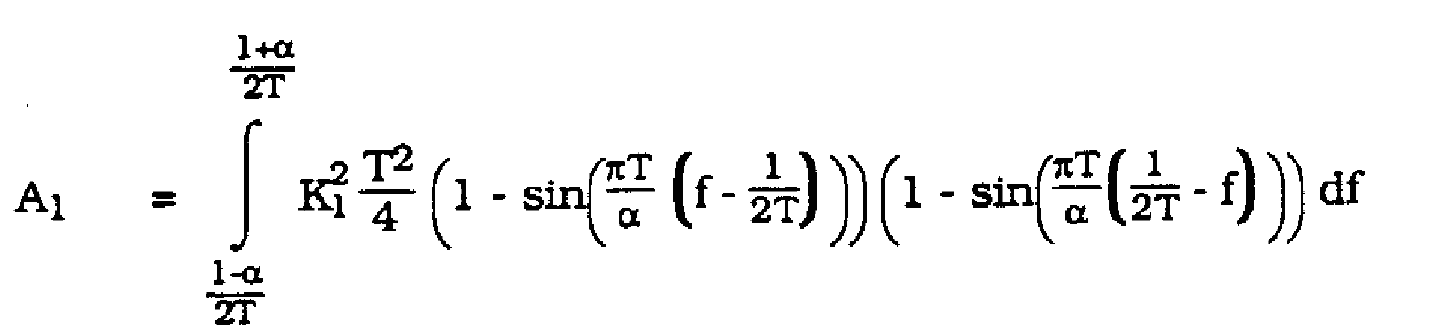 (9)
(9)
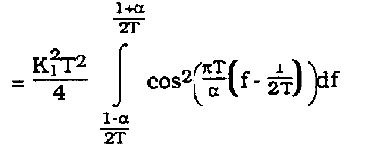 (10)
(10)
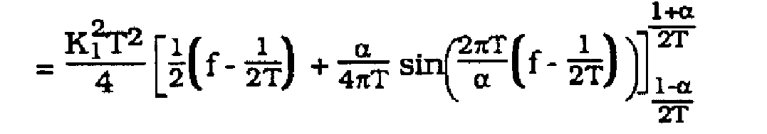 (11)
(11)
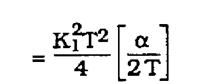 (12)
(12)
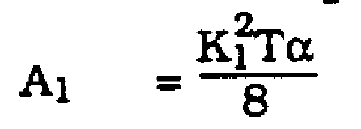 (13)
(13)
For systems where no prefilter is included, timing jitter will vary proportional to ![]() �
�
Systems with little to no excess bandwidth cannot use this technique for timing recovery.
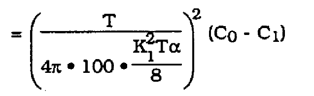
Figure 4 shows the timing wave for the topology shown in Figure l where a prefilter is included. Excess bandwidt: 100% (alpha = 1.0). As can be seen, the variation in the zero crossing phase is small. Figure 5 shows the corresponding case where the prefilter has been removed. Here jitter variance is more noticable. For both cases, the gain of the filter H2(f) at f=1/t=1000 Hz was determined to equal 100.0. Also, ![]() is identically one, and K1=9.14 was determined experimentally.
is identically one, and K1=9.14 was determined experimentally.
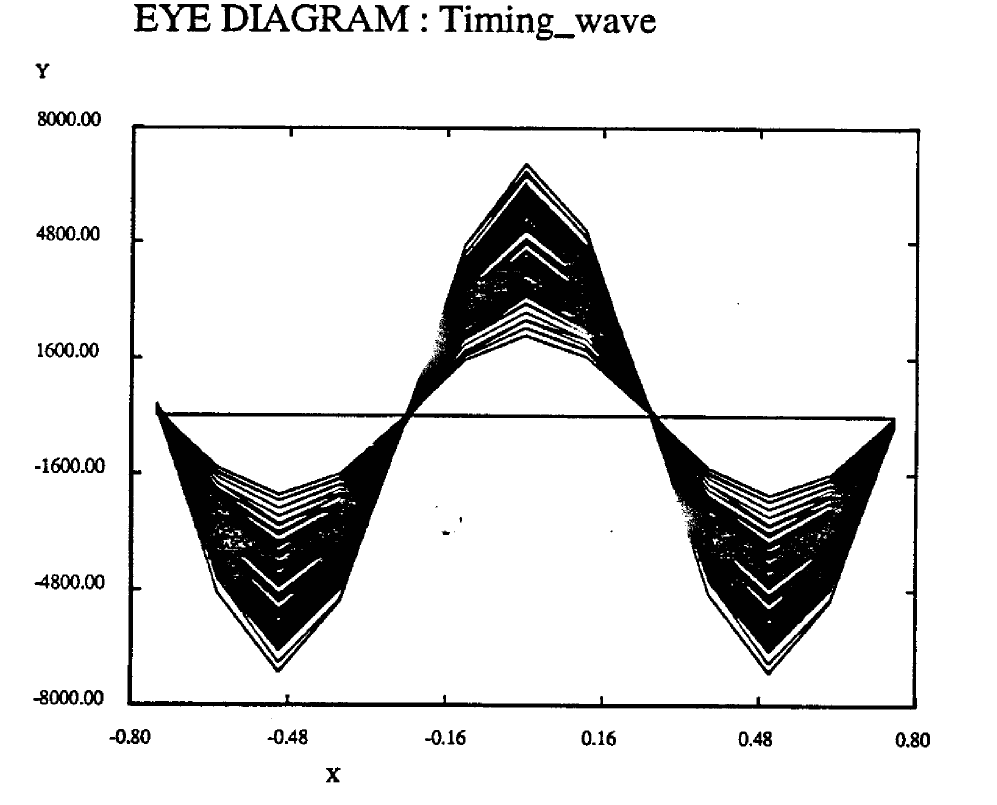
Figure 4 Timing Wave With Prefilter
 (14)
(14)
The theorical prediction for jitter variance is then given by (15), (16), (17) and (18).
 (15)
(15)
 (16)
(16)
 (17)
(17)
 (18)
(18)
Table 1 lists the theoretical and predicted jitter variances.
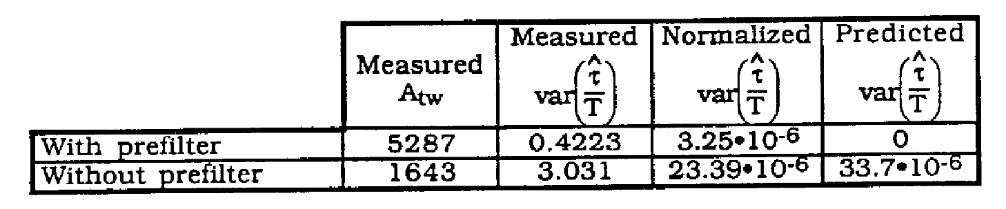
Table 1 Jitter variance without prefilter, alpha=1.0, Q parameter=0.99
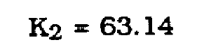
Here the predicted value for ![]() without prefilter is derived by dividing a proportionality constant by the amplitude squared of the timing wave, the proportionality constant K2 being derived from the case with prefilter.
without prefilter is derived by dividing a proportionality constant by the amplitude squared of the timing wave, the proportionality constant K2 being derived from the case with prefilter.
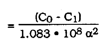
A baseline figure for (C0-C1) can be calculated from the case without prefiltering
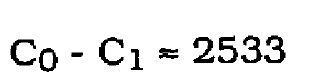 (20)
(20)
It should be mentioned that no bit errors were observed for either case. For both cases, a delay of -20 was observed in the generation of a timing clock. For both cases, the timing clock did not stablize until after 90 bits.
The relationship between timing wave amplitude, timing Jitter and excess bandwidth are given in (7), (8) and (13). Here the system was simulated for various values of excess bandwidth. No prefilter is used. The timing jitter is predicted using both the baseline figure for (Co - C1) given by (20), and also by (19). where K2 is determined for the case alpha = 1.0, no prefilter.
 (21)
(21)
This allows one to see how jitter variance varies with measured vs. predicted timing wave amplitude. Table 2 lists the simulation results.
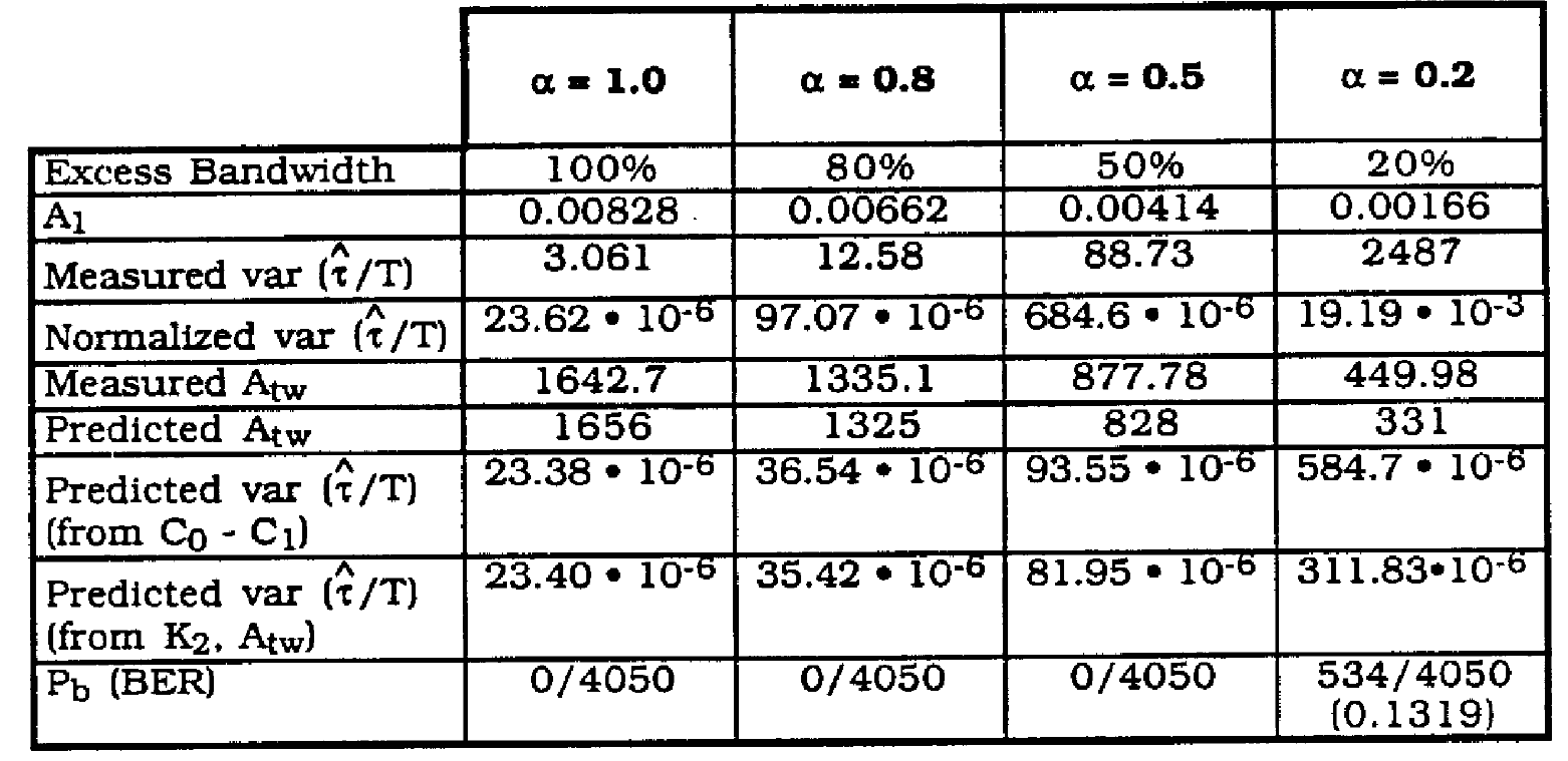
Table 2 Jitter variance vs, excess bandwidth
Predicted Atw, is given by (22)
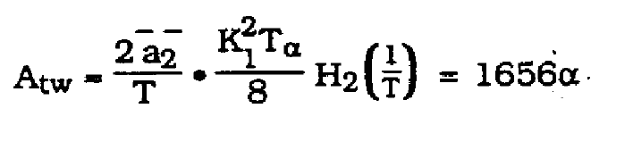 (22)
(22)
For these cases. the Q parameter= 0.99, resulting in H2(1/T) = 100.
Predictions for the amplitude of the timing wave are very accurate for alpha > 0.2. This explains the close correlation between the two techniques for predicting  since one relies on the predicted timing wave amplitude and the other on the measured value.
The predictions for timing variance do not match, the measured results. The jitter variance increases much more rapidly than ![]() and starts to increase by
and starts to increase by ![]() · This is most likely due to the improper assumption of (Co -C1) relationship being fixed. More accurate predictions whould have to take the relationship with C0, C1 and excess bandwidth into account.
· This is most likely due to the improper assumption of (Co -C1) relationship being fixed. More accurate predictions whould have to take the relationship with C0, C1 and excess bandwidth into account.
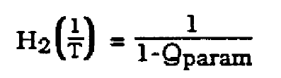
No bit errors were observed until alpha = 0.2. Figure 6 shows the timing wave for this case. For a measured of 19.2 • 10^-3, the resulting sigma would equal 0.14/T. It is then clear why bit errors would be appreciable. For Nyquist pulse shaping, sampling amplitude is sensitive to sampling phase. As excess bandwidth decreases, the sensitivity to sampling phase increases. Even with prefiltering, a PAM system With alpha = 0.2 would demonstrate more bit errors than for larger alpha.
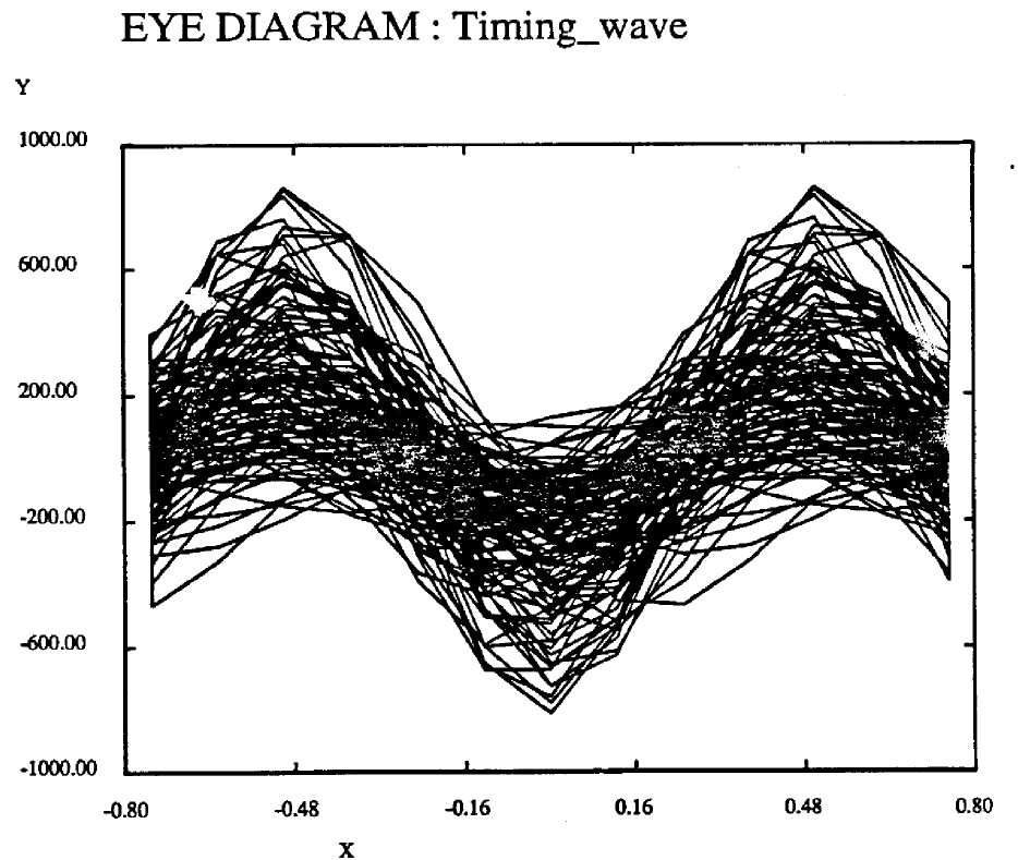
Figure 6. Timing Wave for No Prefilter alpha = 0.2
The performance of the timing recovery system in terms of additive noise and bandpass filter Q are examined next. No predictions for jitter variance are given since no easily evaluated expression for Jitter variance in terms of additive noise were found. For these simulations. excess bandwidth of 100% is used, and a prefilter is included. Jitter variance without additive noise should theoretically be zero.
The gain of the bandpass filter H2(f) in terms of the Q parameter was determined experimentally to obey (23).
 (23)
(23)
The resulting Q values for H2(f) when Qpar = 0.9, 0.99, 0.999 were not determined. For larger Qpar, the gain of H2(f) increases. For a system without prefiltering. this is advantageous since the Jitter variance is inversely proportional to the square of the timing wave amplitude. For a system with a prefilter and additive noise, higher bandpass gain should not improve performance. Higher bandpass Q should improve performance, however, since the noise bandwidth is reduced.
Table 3 gives the results of simulations for Qpar = 0.9. 0.99. 0.999 and additive channel noise ![]() = 0, 0.05, 0.5.
= 0, 0.05, 0.5.
Timing wave amplitude scales roughly with the bandpass gain H2 ( 1/T) for each case. For the case of Qpar = 0.9, appreciable jitter variance exists even when ![]() = 0. Figure 7 shows the timing wave for this case. For
= 0. Figure 7 shows the timing wave for this case. For ![]() = 0.5. appreciable bit errors are occurring.
= 0.5. appreciable bit errors are occurring.
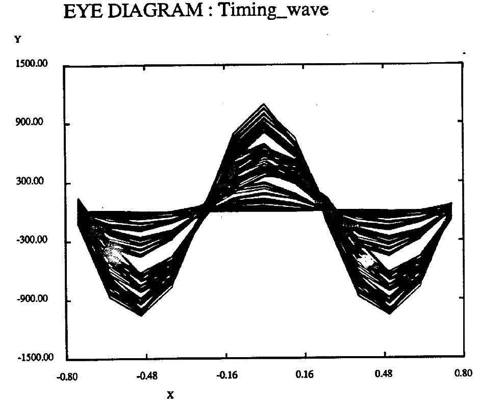
Figure 7. Timing Wave for Qpar • 0.9, ![]() =0
=0
For the case where Qpar = 0.99. 0.999. Jitter variance isn't excessively large, even with large ![]() • Figure 8 shows the timing wave when Qpar = 0.999,
• Figure 8 shows the timing wave when Qpar = 0.999, ![]() = 0.5. Timing Jitter appears insignificant (sigma = 0.0098). It is interesting to note that the Jitter variance appears to increase almost linearly with
= 0.5. Timing Jitter appears insignificant (sigma = 0.0098). It is interesting to note that the Jitter variance appears to increase almost linearly with ![]() as
as ![]() varies from 0.05 to 0.5. This suggests that jitter variance is directly proportional to additive noise.
varies from 0.05 to 0.5. This suggests that jitter variance is directly proportional to additive noise.
Figure 9 shows the recovered timing sample signal for the case where Q = 0.999, ![]() = 0.
= 0.
Figure 8. Timing Wave for Qpar =- 0.999,  = 0.5
= 0.5
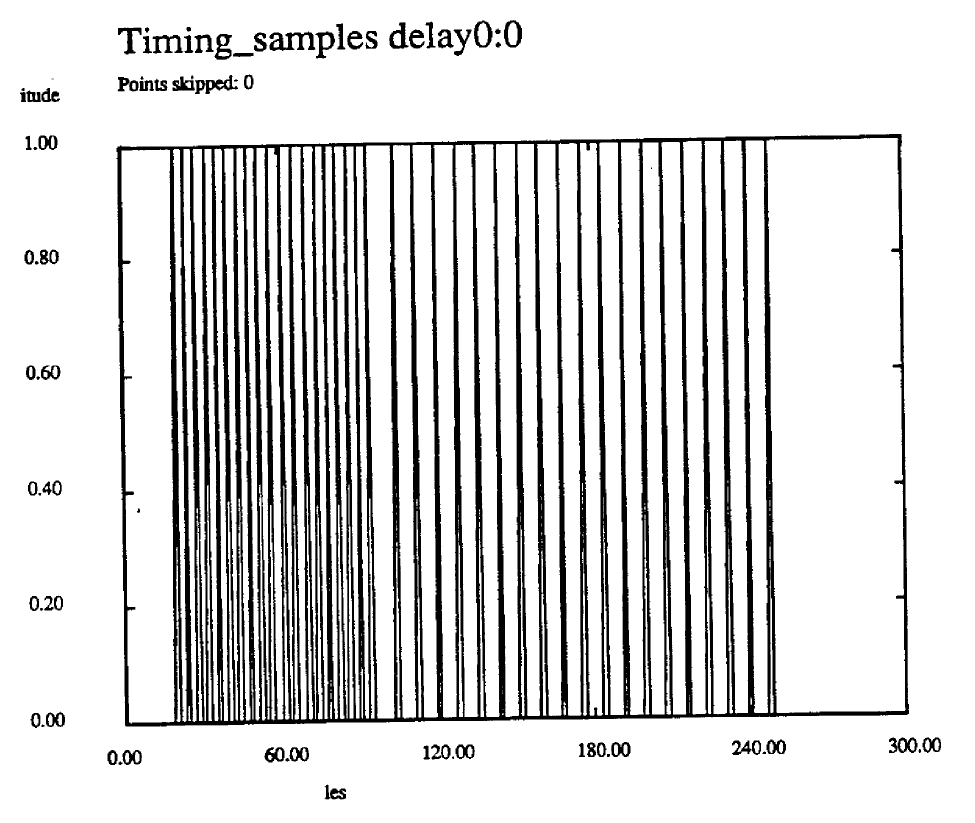
Figure 9. Recovered Timing Samples Qpar • 0.999 = 0.05
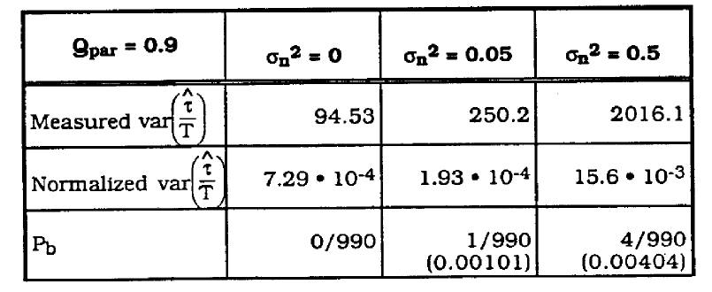
Table 3. Jitter variance vs Qpar
Significant differences in the transient behavior for this signal for fixed additive noise varying in the Qpar was not observed. What was observed was that increasing additive noise from ![]() = 0 to
= 0 to ![]() = 0.05 caused the timing samples to begin sooner and settle into a stable state sooner. Without additive noise, the timing samples usually started at bit 20 and settled by bit 90.
= 0.05 caused the timing samples to begin sooner and settle into a stable state sooner. Without additive noise, the timing samples usually started at bit 20 and settled by bit 90.
The delay is due to delays in the pulse shaping filter, prefilter and bandpass fileter. With additive noise, the timing samples started at bit 126 and settled by bit 50. A possible explanation for this behavior is that the statistics of the data signal for the first few bits are correlated and are not "white" enough to prevent a significant spectral content at fs=1/2T at the input of the squarer. Additive noise "fires up" the timing circuitry faster, Also, the uncorrelated nature of the noise help the timing samples to settle faster.
The results from Table 2 indicate that a high Q bandpass filter is desirable. One trade-off to using a high Q filter is that perfrormance can deteriate drastically if the filter is not tuned precisely to f=1/2T.
Figure 10 shows the topology for a non-ideal transmission channel. The channel has a lowpass filter to approximately simulate the lowpass characteristic of most transmission channels (i. e. twisted pair. coax). The dual paths with gain and delay modeling multipath reflection are often encountered in twisted pair channels from bridged taps or in microwave systems from reflections off water, buildings, etc. The addnoise block models additive white Gaussian thermal noise always encountered in transmission channels. Adjusting the channel parameters can result in a channel with severe distortion.
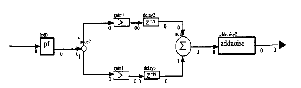
Figure 10. Transmission Channel With Optimal Low-Pass Characteristic, Multi-Path Distortion and AWGN
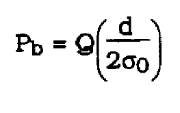
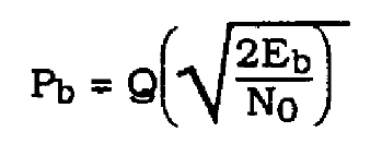
In this section, the theoretical bit error rate (BER) of a PAM system is compared to simulated results. The topology used closely resembles that shown in Figure 1 without the timing recovery subsystem. The probability of bit error (Pb) for a binary PAM system is given by
 (24)
(24)
where d is the distance between possible sample points and ![]() is the AWGN at the sampling point which equals the noise variance at the output of the matched filter. Pb can also be expressed by
is the AWGN at the sampling point which equals the noise variance at the output of the matched filter. Pb can also be expressed by
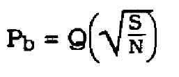 (25)
(25)
where
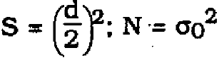 (26)
(26)
An important figure of merit is to calculate Pb in terms of the noise power in the channel. For AWGN. the power spectral density of noise can be expressed by:
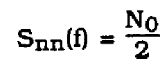 (27)
(27)
The noise power in a channel of bandwidth W is
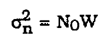 (28)
(28)
For the system simulated, the sampling rate is 80,000 Hz resulting in a bandwidth W of 40,000 Hz. The noise power at the output of the matched filter is shown by Sklar in [4] as
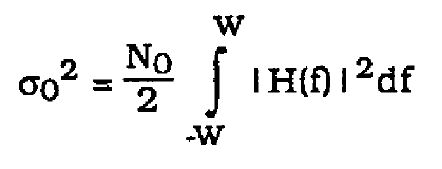 (29)
(29)
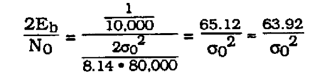
For this system,
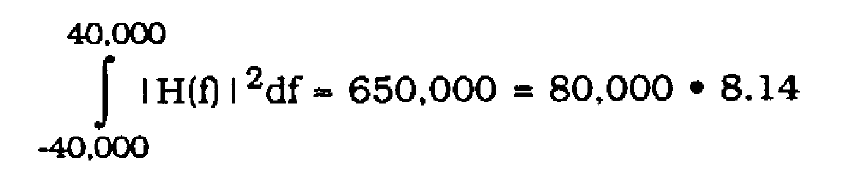 (30)
(30)
was determined experimentally. Then
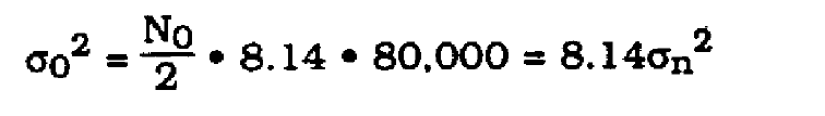 (31)
(31)
The probability of bit error can be given by
 (32)
(32)
where
 (33)
(33)
is the energy per transmitted bit (the pulse shaping filter preserves unit bit energy).
Finally,
 (34)
(34)
where 63.92 was determined to be the signal power S at the sample point.
Table 4 compares measured Pb versus SNR and predicted Pb. Figure 11 is a plot of these values. As can be seen, there is close correlation between the theoretical and measured results.
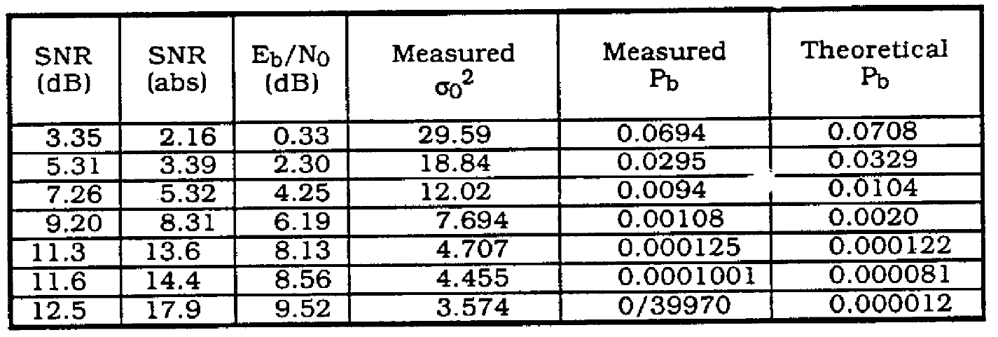
Table 4. Pb vs SNR
For this section, a channel with a lowpass response is analyzed. The impulse repsonse of the channel is given in terms of a pole paramater alpha.
 (35)
(35)
This results in a z-transform
 (36)
(36)
and a DFT response
 (37)
(37)
where
 (38)
(38)
The magnitude of ![]() is given by
is given by
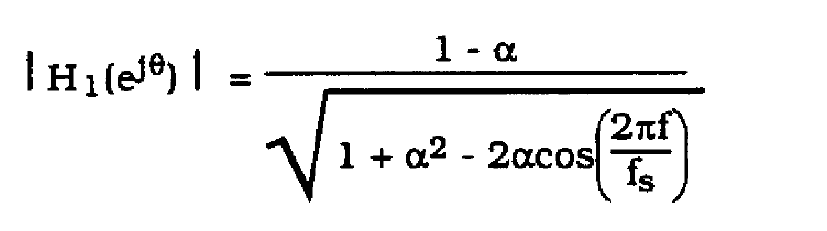 (39)
(39)
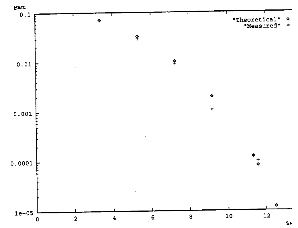
Figure 11. Pb versus SNR (dB)
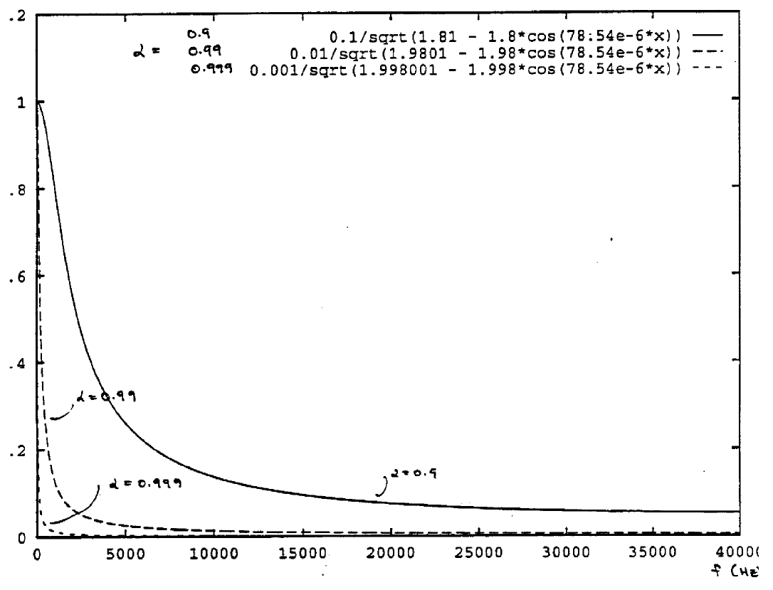
Figure 12. Lowpass Filter Magnitude Response
The response is plotted in Figure 12 for a = 0.9. 0.99. 0.999. As can be seen, for alpha = 0.99, 0.999 the channel exhibits severe attenuation in the bandwidth of 10.000 Hz which is the data rate for the simulated PAM system.
A digital filter that could compensate for the channel lowpass characteristic would be an FIR "forward" filter, often referred to as an all-zero filter since the filter frequency response consists of all zeroes. Ideally, one would like to design an adaptive filter which could adjust its tap weights to compensate for variations in the channel characteristics.
Figure 13 shows the topology used for simulations of the lowpass channel equalizer. Figure 14 shows the adaptive filter equalizer designed for this simulation. An eighth-order fractionally spaced fast transversal filter (FTF) was chosen as the adaptive filter. The two filter channels are fed by a sampler that samples at the Nyquist rate (twice the baud rate). Each channel is a baud rate filter. The FTF filter implements a general order recursive least squares (RLS) filter algorithm. The filter output is at the baud rate. The filter output is fed to a comparator (slicer) to determine whether a +a or -a symbol was sent. The filter weights are updated by the difference signal between the output and the sliced signal. The filter is trained by the original bit sequence for 32 bits, and then the filter switches to its own sliced output to calculate the error signal. The RLS parameter was chosen as 1.0.
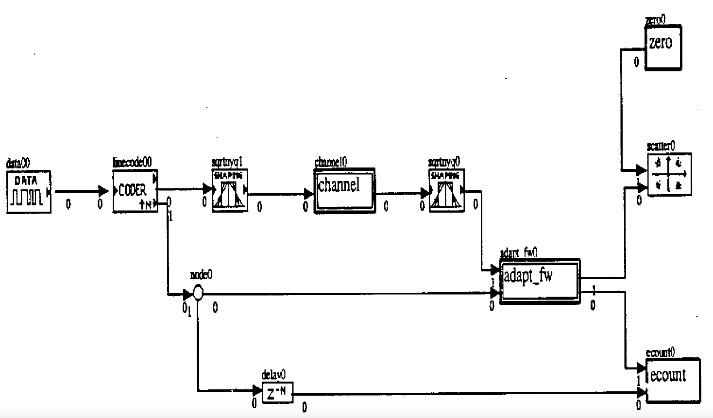
Figure 13. Topology for Lowpass Channel Equalizer
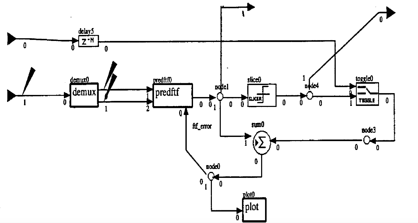
Figure 14. Adaptive Equallzer for Lowpass Channel Two-Channel Fractionally Spaced Fast Transversal Filter lambda= 1.0
The RLS adaptive filter was chosen due to its superior convergence properties and excess error properties. An N-th order RLS filter generally converges on O{N) iterations, and has excess error ~0 when lambda = 1.0. The
order of 8 and lambda = 1.0 where chosen as an optimal match of filter complexity and performance. Choosing lambda = 1.0 yielded the lowest error signal power for all cases tested. An order eight filter yielded the best error power performance of the orders tested (6 - 12}. The training sequence length of 32 was chosen as a best compromise between filter convergence behavior and system delay (from training). Figure 15 shows the typical convergence behavior of the error signal. Choosing lambda = 1.0 results in a filter that is less stable than for lambda < 1. The performance of this equalizer in the presence of noise is described later.
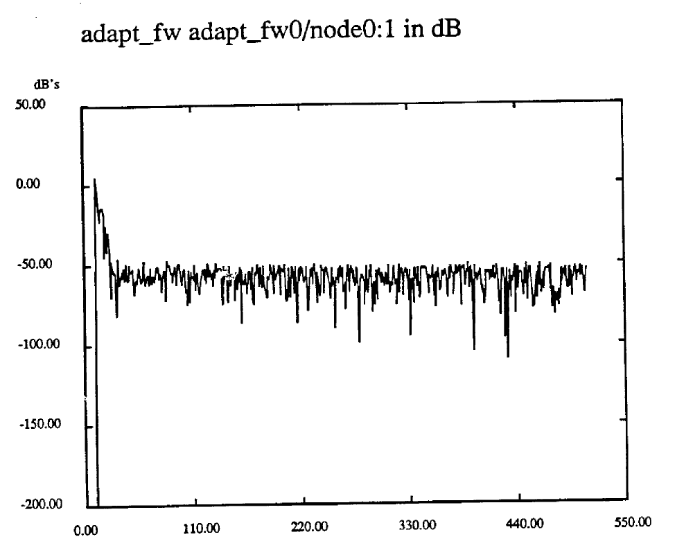
Figure 15. Convergence of Pre-dftf Error Signal, alpha • 0.99, = 0
A fractionally spaced equalizer was chosen due to the uncertainty in desired sampling phase for a signal with severe ISI as will be the case with the lowpass channel simulated. Figure 16 shows the received signal at the
sampler with alpha = 0.999. Figure 17 and Figure 18 show the corresponding sample values for each received baud. The sample times are 1/2T apart, or half the baud period. Note that each sampler produces samples at the baud rate. It can be seen that there is substantial energy for each bit at both sample points.
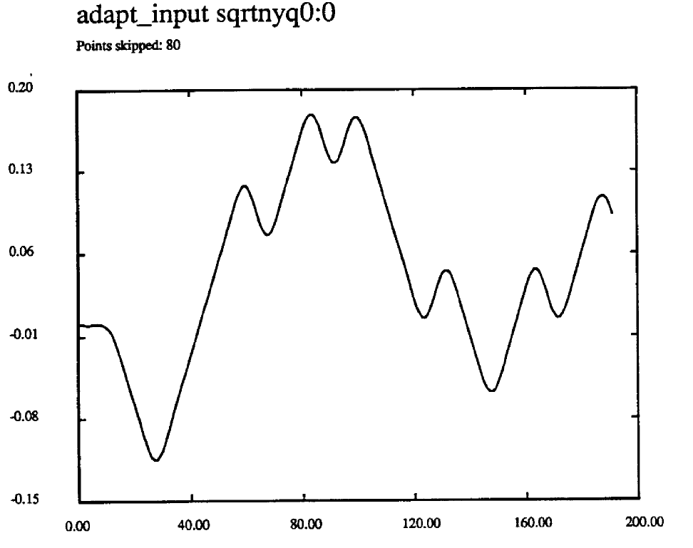
Figure 16. Received Signal at Sampler alpha= 0.999
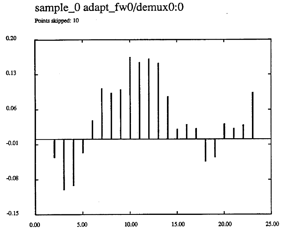
Figure 17. Sample Values at Channel 1, alpha= 0.99
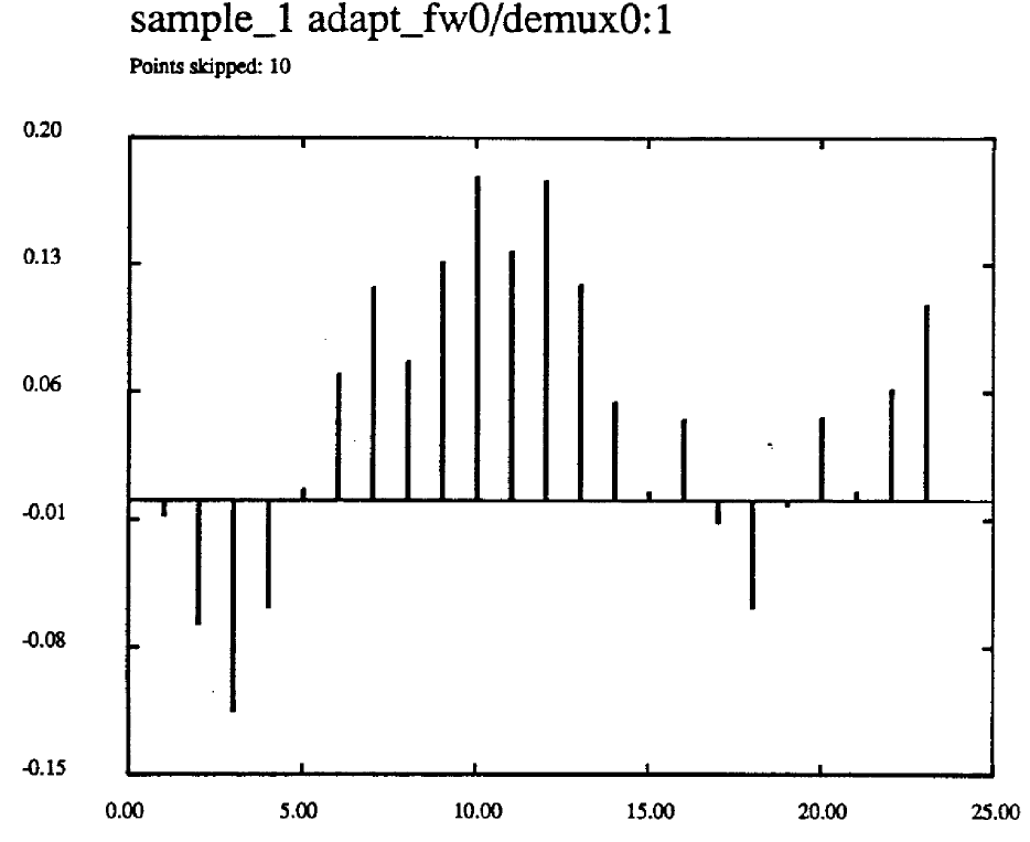
Figure 18. Sample Values at Channel 2 alpha= 0.99
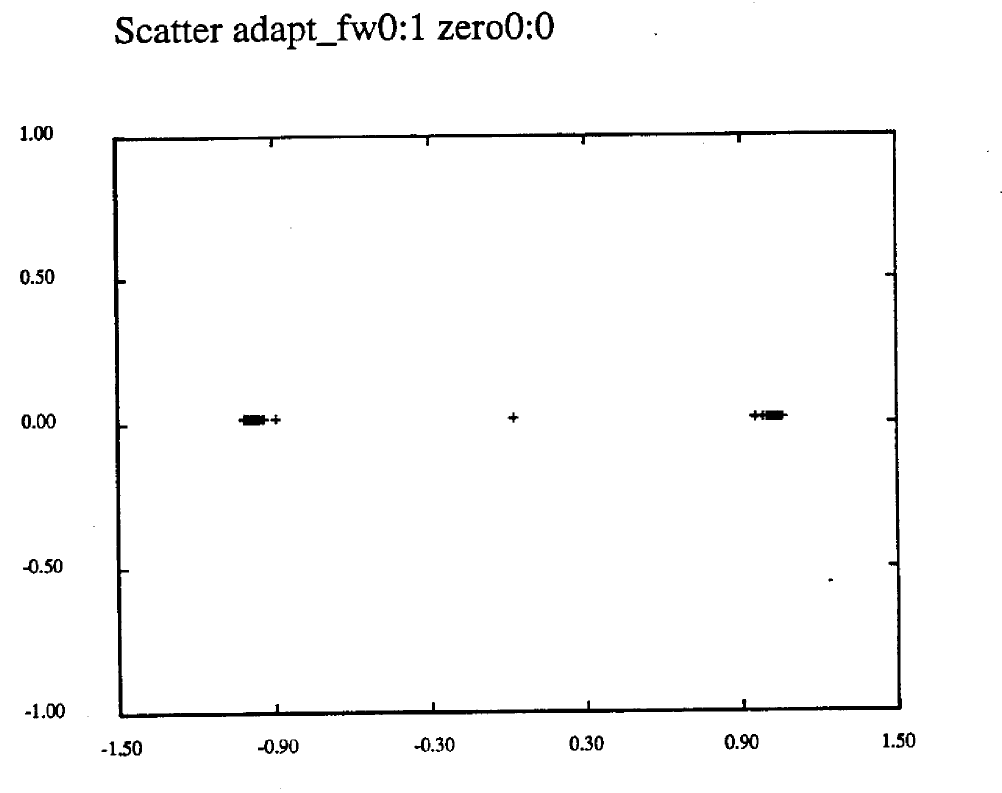
Figure 19. Scatter Diagram for Lowpass Channel Equalizer alpha=0.999 ![]() =0
=0
In [5], Qureshi shows that a fractionally-spaced equalizer is insensitive to timing phase. This is partly due to the fact that sampling at >= 2/T . prevents aliasing at the sampler. For a channel with severe ISI, it would be difficult to design an adaptive filter with baud rate sampling that could adjust its sampling phase to prevent sampling errors.
Table 5 shows the filter channel input powers and filter error power for alpha = 0, 0.9. 0.99. 0.999. For each case, the additive noise is zero. No bit
errors were observed. The worst case scatter diagram (alpha = 0.999) is shown in Figure 19. It is clear from these results that the equalizer performed extremely well when no channel noise was added.
(4096 points taken. 32 skipped)
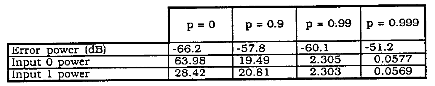
Table 5. Performance of lowpass channel equalizer
The frequency response of the multipath channel is determined from the difference equation.
 (40)
(40)
This results in the z-transform
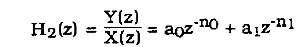 (41)
(41)
The resulting frequency response is:
 (42)
(42)
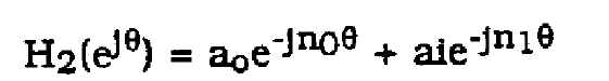
Let no = o. DELTA = n1 - no = n1. Then within a frequency independent delay term
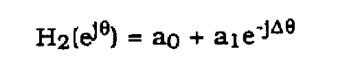 (43)
(43)
and
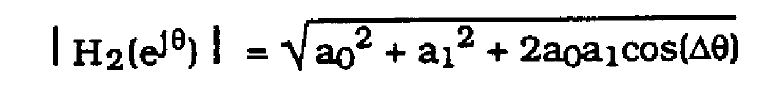 (44)
(44)
where theta obays (38). Assuming a0=1
 (45)
(45)
This frequency response will have periodic nulls occurring where
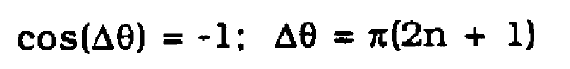 (46)
(46)
It is desired to simulate the system where the nulls occur at f = 5000 Hz. Then
 (47)
(47)
and
 (48)
(48)
Figure 20 shows a plot of ![]() where DELTA = 8 and a0 = 1, a1 = 0.2, 0.8. 0.99.
where DELTA = 8 and a0 = 1, a1 = 0.2, 0.8. 0.99.
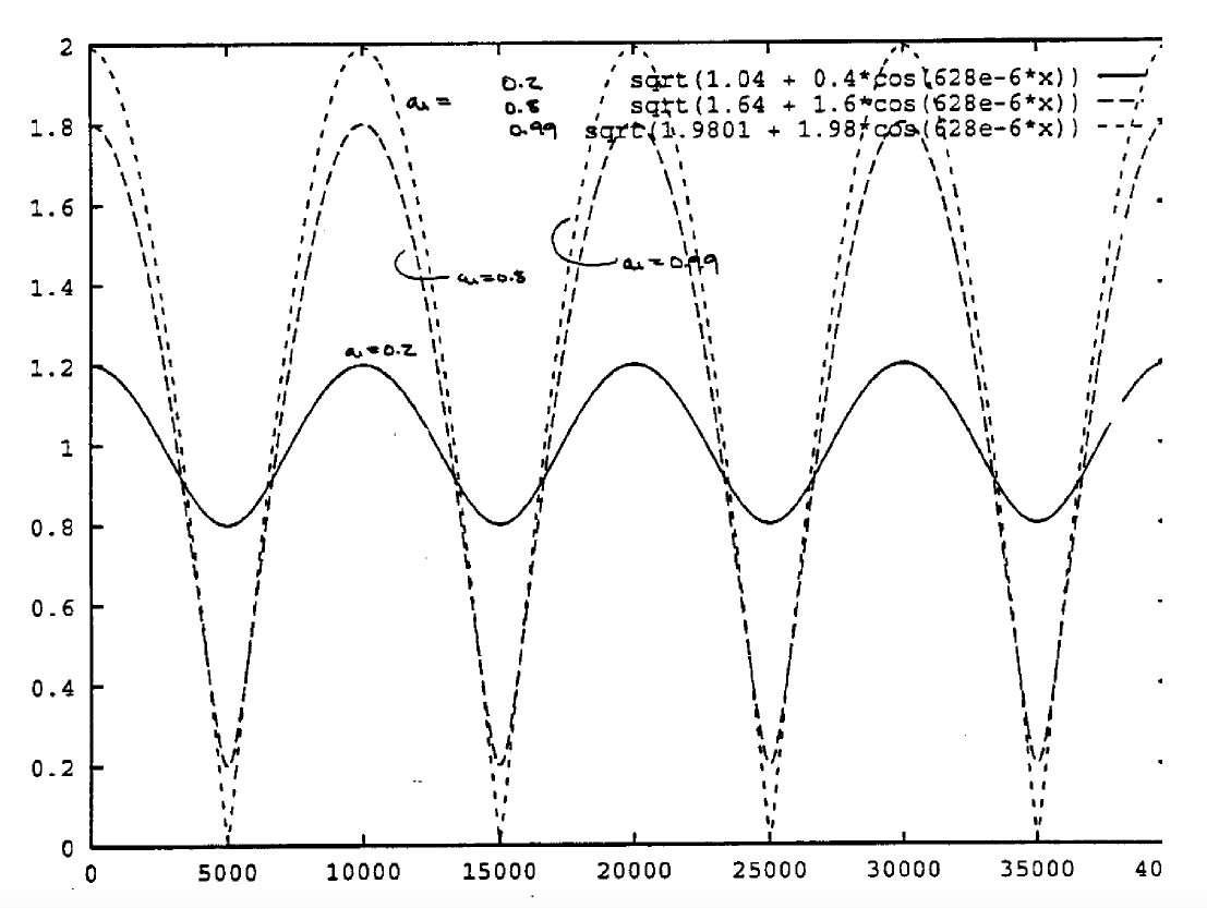
Figure 20. Plot of Multipath Spectral Response
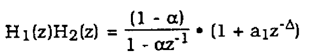
For this section, it is required to design an equalizer to compensate for a lowpass pole of 0.9 and multipath distortion for a1 = 0.1, 0.2, 0.8, 0.99. The frequency response of this channel would be obtained by evaluating the product ![]() . Figure 21 is a plot of the impulse response of this channel for alpha= 0.9, a1 = 0.99.
. Figure 21 is a plot of the impulse response of this channel for alpha= 0.9, a1 = 0.99.
The z-transform of this channel is given by
 (49)
(49)
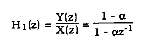
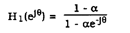
where the delay term ![]() is at the sampling rate of 80,000 kHz. In Section 2.2, an appropriate equalizer for H1(z) was shown. That FIR filter would be unable to compensate for H2(z) since it is an all-zero filter. For Delta = 8, H2(z) can be killed by a filter With response
is at the sampling rate of 80,000 kHz. In Section 2.2, an appropriate equalizer for H1(z) was shown. That FIR filter would be unable to compensate for H2(z) since it is an all-zero filter. For Delta = 8, H2(z) can be killed by a filter With response
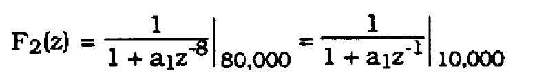 (50)
(50)
an IIR filter of order 1. Such a filter can be implemented as feedback FIR filter.
In [5], Qureshi discusses a popular equalizer structure known as a decision feedback equalizer (DFE). In this system, a feedback FIR filter is fed by bit decisions from the slicer. The feedback filter subtracts either its positive or negative impulse response from the signal at the input to the forward filter.
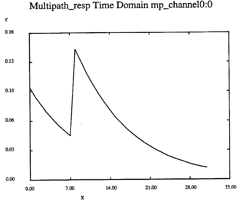
Figure 21. Impulse Response of Multi-Path Channel with Lowpass Response a=0.9 and a1=0.99
The feedback is capable of cancelling zeroes in the spectrum of the input signal. It is also capable of improving the ability of the forward filter to cancel poles, since the forward filter is no longer forced to attempt to drive the overall system impulse response to an impulse, i. e. the forward filter no longer requires as much high-frequency gain.
Figure 22 shows the topology for the adaptive equalizer designed to equalize the channel with lowpass and multipath characteristic. Figure 23 shows the DFE designed. The feedback path is implemented as a fourth-order channel in the Fast Transversal Filter (fast RLS adaptive filter). Both forward and feedback paths are updated with the same error signal.

Figure 23. Decision Feed.back Equalizer
Two Channel Fractionally-Spaced FTF Forward Filter
One-Channel Feedback Path
lambda= 1.0
Table 6 tabulates the result for the DFE for alpha = 0.9, a1 = 0.1. 0.2. 0.8. 0.99. For each case, the additive noise is zero. The FTF error signal showed rapid convergence as in Figure 15. Figure 24 shows the worst-case signal at the sampler, for the case when a1 = 0.99. Substantial ISI 1s evident. For the cases examined, no bit errors were observed. The worst case scatter diagram, for a1 = 0.99. is shown in Figure 25. The error power for each case is extremely low, though it is growing when a1 = 0.99. The DFE appears to equalize the channel very well when no additive noise is present.
Figure 24. Received Signal at Sampler alpha=0.9 a1=0.99
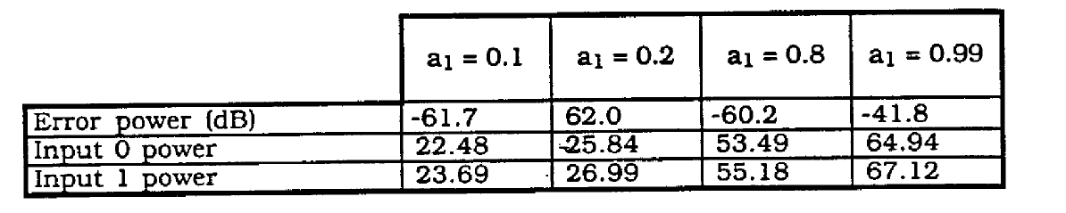
Table 6. Performance of-DFE equalizer
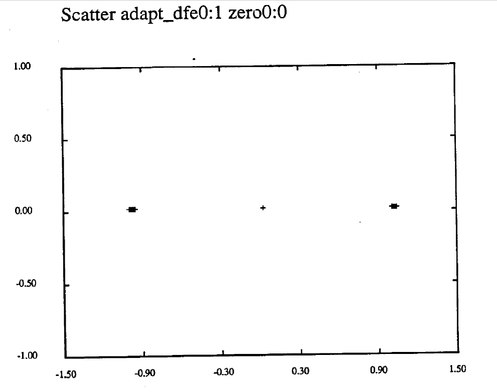
Figure 25. Scatter Diagram for Lowpass and Multi-Path CbaunP-1 Equalizer alpha=0.9 a1=0.99
It is interesting to examine the resulting tap weights for the DFE after convergence. Table 7 lists the DFE tap coefficients for the case when alpha = 0.9. a1 = 0.99. Table 8 lists the tap coefficients when alpha = 0, a1 = 0.99. For both cases. adjacent pairs of weights are approximately the negative of each other. In (50) it was proposed that the multipath distortion could be cancelled by one tap. The same cancellation is achieved when the tap weight magnitudes are equal and they alternate in sign. The feedback filter attempts to distribute energy as evenly as possible over the tap weights. In Table 7, it is clear that the feedback filter is helping the forward filter to cancel the pole.
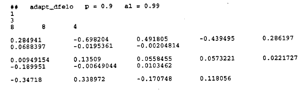
Table 7 DFE Tap Weights After Convergence alpha=0.9 a1=0.99
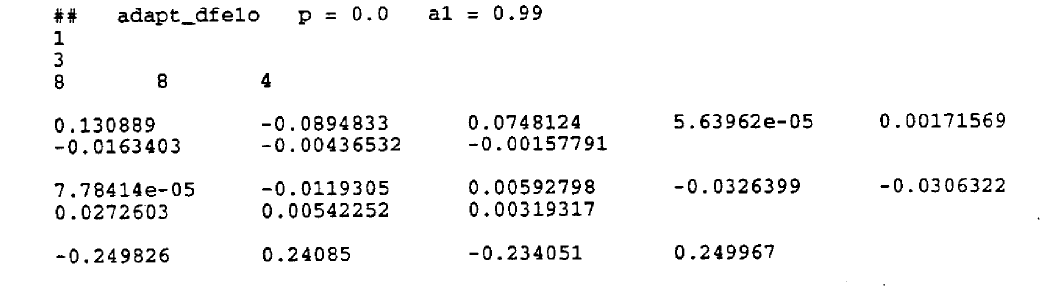
Table 8. DFE Tap Weights After Convergence alpha=0 a1=0.99
An important figure of merit is the performance of the adaptive equalizers in the presence of additive noise in the transmission channel. It is known that additive noise in the received signal will affect the updating of the adaptive filter tap weights. For RLS filters, the noise is cancelled at a very slow rate. One measure of performance is to compare the performance of the equalizer system with no channel distortion to a PAM system with no equalization.
It was determined that an SNR of 25.5 dB at the sampler will result in a Pb = 0.0007 and an output error power of -15.53 dB for the forward filter system. For the DFE. a Pb = 0.0175 occurs for SNR =28.52 dB and error power = = -17.5 dB. These error values are much worse than for nonequalized systems. The likely cause of this behavior is that the equalizer is trying to drive the overall system impulse response to be an impulse. This results in a high-pass filter response which will emphasize noise. The DFE system is much more susceptible to additive noise (3 dB) than the forward filter system. This is probably due to the fact that errors in the predicted bit propagate through the DFE.
Both systems exhibited a threshold effect on the BER. If SNR was decreased by less than 1 dB, the BER increased rapidly. However. the FTF error power does not exhibit this threshold effect. Despite initial first impressions, the FTF error power is not a good means of predicting BER for the adaptive equalizers.
Error performance with channel distortion is also important. For the forward filter system, Pb = 0.0022 is observed for alpha = 0.99. and SNR 33.6 dB. This is worse than for the case of the clean channel. That is intuitive since the forward filter will adapt to a more highpass _response in this case. Pb = 0.44 is observed for alpha = 0.9, a1 = 0.99 and SNR = 38.13 dB for the DFE. For SNR = 38.35 dB. no errors are observed.
It can be concluded that adaptive equalizers are very sensitive to additive noise and will likely not perform in environments with SNR < 28 dB. The DFE shows more sensitivity to additive noise than the forward filter. In either case, it should be noted that the BER for the distorted channel without equalization ~0.5. The equalizers are necessary for any possible data transmission at high bit rates over these channels. Figure 26 shows DFE
scatter response, SNR = 38.17 dB. Pb = 0. alpha = 0.9. a1 = 0.99.
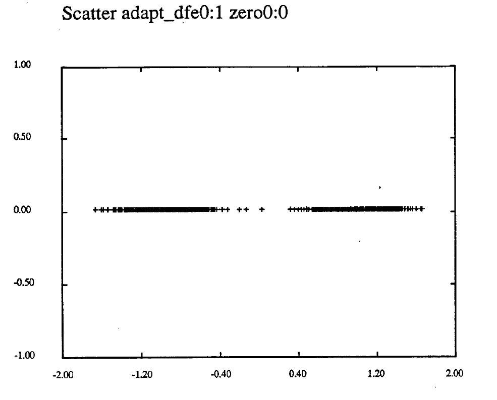
Figure 26. DFE Scatter Plot SNR = 38.17 dB
alpha = 0.9 a1=0.99
1- L. E. Franks and J. P. Bubrouski, " Statistical Properties of Timing Jitter in a PAM Timing Recovery Scheme." IEEE Transactions on Communications, vol. COM-22, no. 7, pp. 913-920, July 1974.
2- L. E. Franks, "Carrier and Bit Synchronization in Data Communication - A Tutorial Review,'' IEEE Transactions on Communications. vol. COM-28. no. 8, pp. 1107-1121, August 1980.
3- G. L. Cariolaro and F. Todero, "A General Spectral Analysis of Time Jitter Produced in Regenerative Repeater," IEEE Transactions on Communications, vol. COM-25. no. 4. pp. 417-426, April 1977.
4- B. Sklar, Digital Communications. Englewood Cliffs. New Jersey. Prentice Hall. 1988.
5- S. U. H. Qureshi. "Adaptive Equalization," Proceedings of the IEEE. vol. 73. no. 9, pp. 1349-1387, September 1985.
| © 2007-2017 Silicon DSP Corporation |
|---|