| CCSP | Silicon DSP Corporation | CCSP Tech Blog |
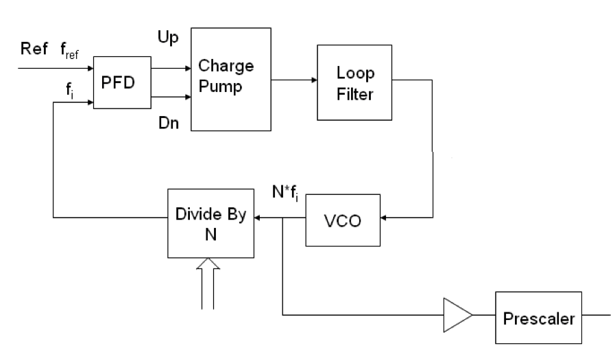
It is imperative to have a high level behavioral model of the PLL in order to verify the operation of the PLL and to do extensive “what if” scenarios and fine tune the design parameters. The high level block diagram of the PLL is shown in below:
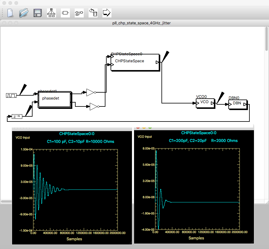
A block diagram level simulator for Capsim¨ was written in C which allows for very fast simulations and the verification of PLL performance. This is based on a Capsim¨ phase-frequency detector and charge pump block diagram simulation by the author’s Ph.D. Student, Ray Kassel in 1990 at NC State University. The original application note can be seen here ![]() .
.
The preliminary goal is to match the nonlinear mixed analog/digital PLL circuit perfromance with high level fast "C" modeling of the charge pump PLL.
| Technical Papers on Charge Pump PLLs | Capsim V7 (Qt) Modeling and Simulation of Charge Pump PLL (4 GHz) |
|---|---|
1- PLL Charge Pump Analysis 2- Charge Pump Modeling Solution 3- CapsimTMK Charge Pump PLL Project (Zipped File) |
 |
| © 2007-2017 Silicon DSP Corporation |
|---|